Monolithic Power Systems (MPS) MP2650 Battery Management Buck/Boost Charger ICs
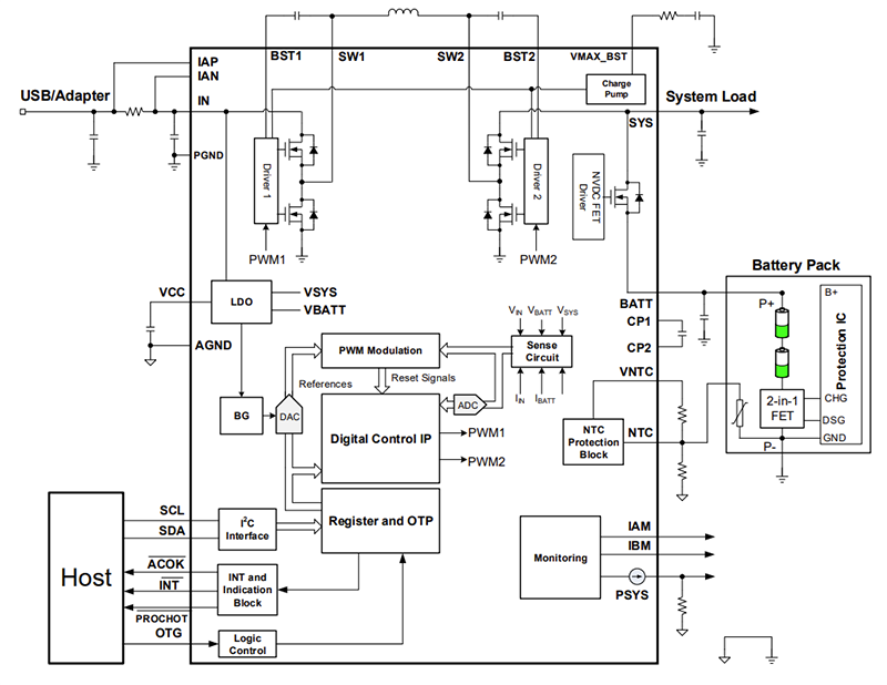
Monolithic Power Systems (MPS) MP2650 Battery Management Buck/Boost Charger ICs offer USB On-the-Go (OTG) and narrow-voltage DC (NVDC) power path management for battery packs with 2 to 4 cells in series. All power MOSFETs are integrated, providing a compact system solution size. The QFN-30 (4mm x 5mm) packaged MP2650 accepts a broad input charging voltage (VIN) range (21V maximum). The MP2650 ICs feature two operating modes during the charging process: boost and buck, depending on VIN and the cell count.An I2C interface allows flexible configuration to set the parameters in both charging and OTG modes. Parameters include the input current (IIN) limit, VIN limit, charging current, battery charge voltage regulation, and safety charge timer. Status and fault registers provide operation statuses. For safety, the MP2650 limits the die temperature to a preset value of +120°C. Other safety features include input over-voltage protection (OVP), battery OVP, system OVP, thermal shutdown, battery temperature protection, and a configured timer to prevent prolonged charging of a dead battery.
NVDC power path management regulates the system voltage within a narrow DC range, which provides an optimized system bus voltage for the rails at the system bus. This feature allows the system to continue operating even with a depleted or removed battery.
Features
- Buck or Boost charger for battery Packs with 2 to 4 cells in series
- All switching MOSFETs are integrated
- NVDC Power Management with an integrated Battery FET
- 4V to 21V operating input voltage (VIN) range
- Up to 28V (20ns) sustainable VIN
- Configurable VIN limit
- Up to 5A configurable input current (IIN) limit (up to 45W total power)
- Up to 5A configurable charge current
- Configurable battery charge voltage regulation up to 4.5V/cell
- System power indication via the PSYS pin
- IIN and battery current monitoring via the IAM and IBM pins
- Input Over-Voltage Protection (OVP), battery temperature protection, battery OVP, and system OVP
- Configurable safety charge timer
- Thermal regulation and shutdown
- 600kHz, 800kHz, 1MHz, or 1.25MHz configurable Switching Frequency (fSW)
- Input power source status indication pin
- I2C interface to support flexible parameter control
- Comprehensive fault and status reporting in register
- Up to 5V/3A USB On-The-Go (OTG)
- Configurable OTG Output Current (IOUT) limit
- Short-Circuit Protection (SCP) in OTG mode
- Available in a QFN-30 (4mm x 5mm) package
Applications
- Tablets and notebooks
- BLUETOOTH® speakers
- Portable gimbals
Specifications
- Recommended operating conditions
- 4V to 21V supply range
- Up to 5A input current
- Up to 5A charge current
- Up to 14A discharge current via battery FET (DC)
- Up to 18V battery voltage
- -40°C to +125°C operating junction temperature range
- 3.29W continuous power dissipation at +25°C
- DC-DC converter
- 9.5mA maximum input shutdown current
- 5mV minimum battery tracking regulation voltage
- 600kHz to 1250kHz typical operating frequency range
- System short-circuit thresholds
- 30mV to 320mV entry
- 110mV to 500mV exit
- Battery charger
- 0.44A to 3.3A fast charge current range
- Trickle charge to pre-charge threshold
- 3.92V to 4.25V range
- 450mV to 650mV hysteresis
- Pre-charge to fast charge threshold
- 6.04V to 6.71V rising range
- 5.85V to 6.54V falling range
- 60mA to 190mA trickle charge current at 1V, 130mA to 240mA at 3V
- 120mA to 1230mA pre-charge current range
- 30mA to 1.75A termination current range
- 100µA typical system power indicator full-scale with 256 steps
- General comparator
- 1.22V typical reference
- 40mV to 180mV hysteresis
- 200Ω typical output open-drain MOSFET resistance
- Battery absent detection
- 1.6V typical threshold
- 10mV typical hysteresis
- Analog-to-Digital Converter (ADC)
- 50kHz typical sample rate
- 10-bit typical resolution
- 1.6V typical reference
- Logic I/O pin thresholds
- 0.4V maximum low-voltage
- 1.3V minimum high-voltage
- 400kHz maximum I2C clock frequency
- Timer
- 4.5MHz to 5.5MHz digital clock range
- 160s typical watchdog timer
- 25.6ms typical short circuit recovery time
- ESD ratings
- 2000V Human Body Model (HBM)
- 750V Charged Device Model (CDM)
Typical Application

Block Diagram


